Demystifying JTAG: A Powerful Tool for Testing and Programming Embedded Systems
Looking for a reliable supplier of JTAG connectors and other electronic components? Look no further than BonChip Electronics. We offer a comprehensive selection of high-quality products from leading manufacturers, along with exceptional technical support and fast delivery.
JTAG (Joint Test Action Group) is a ubiquitous tool in the world of electronics, used extensively for testing, programming, and debugging embedded systems. If you've ever programmed a microcontroller, chances are you've interacted with JTAG or a related standard. But what exactly is JTAG, and how does it work?
The Rise of JTAG: Addressing Testing Challenges
In the early days of electronics, testing circuit boards with numerous input/output (I/O) paths involved cumbersome methods like bed-of-nails test fixtures. As pin density increased and ball-grid array (BGA) packaging became more common, a new solution was needed. JTAG emerged in the 1980s as a standardized approach for testing hardware interconnects between multiple integrated circuits (ICs).
Understanding JTAG Boundary Scan
The core of JTAG lies in boundary-scan technology, defined by IEEE Standard 1149.1. This standard equips each I/O pin on a device with a dedicated logic cell. These logic cells are interconnected, allowing data to be shifted around the chip in one direction. This enables engineers to read or write pin values, facilitating functionality testing.
JTAG also incorporates a test access port (TAP), a logic block responsible for managing data flow and executing tests. The TAP essentially acts as a state machine with several shift registers, allowing it to execute commands like data loading and reading. However, the JTAG framework offers flexibility for manufacturers to add custom commands and logic blocks, expanding its capabilities to include programming and debugging access.
The Evolution of JTAG: From Testing to Programming
So, how did JTAG become synonymous with device programming? Traditionally, programming any device with memory involved addressing a specific word location and then writing data to that address. Early memory devices employed asynchronous addressing schemes with separate data pins for each memory bit. Later advancements included binary decoding for addresses and serial protocols, enabling programmers to communicate with devices using fewer pins.
JTAG's inherent flexibility allowed developers to implement custom logic for programming purposes. The data pipeline provided by the JTAG TAP proved well-suited for programming microcontrollers and FPGAs. Additionally, the standardization of the interface (with some variations across implementations) facilitated consistent device interaction. Further extensions to the standard, like ARM's Serial Wire Debug (SWD), and additional IEEE 1149.x standards broadened JTAG's applicability and utility, shaping it into the versatile tool we know today.
JTAG: A Standard with Flexibility
It's important to note that while IEEE 1149.1 serves as a foundation, it offers considerable flexibility for developers. There are no standard pinouts, connectors, or a vast array of built-in commands. Beyond the basic state machine, many features are optional, including boundary-scan functionality itself. This inherent flexibility allows for variations in JTAG implementations, which we'll explore in future articles.
JTAG Connectors: The Physical Interface
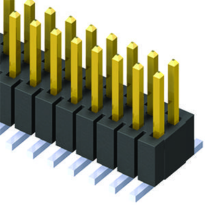
A JTAG connector is essentially a pin header, typically found in either 0.100-inch (2.54 mm) or 0.050-inch (1.27 mm) centerlines. Common configurations include 10-pin (2 x 5), 14-pin (2 x 7), and 20-pin (2 x 10) layouts. JTAG connectors can be through-hole or surface-mount (SMT), shrouded or unshrouded.
While it may seem like a loose standard, it's true that there's no single connector specifically designated for JTAG. In its simplest form, a JTAG connector only requires four or five pins to operate a JTAG TAP. However, designers often incorporate additional ground and signal pins, leading to variations in pin count.
The Test Access Port (TAP)
Figure 1 shows the basic JTAG architecture.
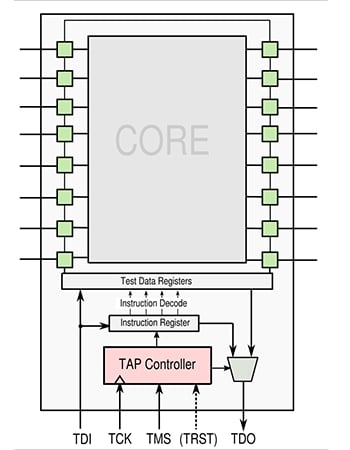
Figure 1. JTAG architecture schematic
Let’s approach this from the basics. The JTAG standard specifies four mandatory signals and one optional signal. All JTAG-compliant devices must include:
- Test data input (TDI) pins
- Test data output (TDO) pins
- A test clock pin (TCK)
- A test mode select pin (TMS) for controlling the TAP state machine
The test reset pin (TRST) is optional in the JTAG standard. It forces the state machine into the reset state. However, this state can also be achieved by holding the TMS pin low and clocking the TCK pin five times.
The TAP Controller
The Test Access Point (TAP) comprises the TAP controller, an instruction register, several test data registers, and some supporting logic. The TAP controller houses the testing state machine and is responsible for interpreting the TCK and TMS signals. The data input pin is utilized for loading data into the boundary cells between the physical pins and the IC core, as well as for loading data into either the instruction register or one of the data registers. The data output pin is used for reading data from the boundary cells or from the instruction or data registers.
The state machine of the TAP controller is controlled by the mode select signal, TMS, which is clocked by TCK. It navigates through two main paths, representing two different modes: instruction mode and data mode. The mode is determined by clocking in a TMS HIGH or TMS LOW bit. Once in a specific mode, the state machine either progresses if TMS is HIGH or moves toward the reset state if TMS is LOW. We will explore the state machine in more detail in the next article.
How to Use JTAG
Working with JTAG typically works as follows:
- First, the instruction mode is selected. One of the states within the instruction mode ‘path’ allows the user to clock in an instruction through TDI.
- Then the state machine progresses until it resets.
- For most instructions, the next step is to select the data mode. In this mode, data is loaded through TDI and/or read from TDO. The data paths for TDI and TDO will be configured in accordance with the instruction that has been clocked in.
- When the read or write operation is complete, the state machine again progresses to the reset state.
Test Instructions and Data Registers
There are two data registers and four instructions which the JTAG standard requires in all devices. Another six data registers and 13 instructions are also standardized, but not required.
The data registers required are:
- BSR – “Boundary-scan register”, the main register for passing data to the boundary-scan cells
- BYPASS – A single-bit pass-thru register, connecting TDI to TDO without first passing through the boundary-scan cells
Vendors can implement other data registers depending on their design needs, whether standardized or design-specific. The only instructions the JTAG standard requires to be implemented are:
- EXTEST – Perform an “external” boundary-scan test using the boundary scan cells
- SAMPLE and PRELOAD – Boundary scan while the device is functional
- BYPASS – Bypasses the boundary scan cells altogether
Common JTAG Instructions
Other recommended instructions include:
- IDCODE – Output an identification code stored in an identification data register
- CLAMP and HIGHZ – Used to isolate parts of the device without risk of damage. HIGHZ forces all logic outputs to high-impedance mode, while CLAMP forces logic outputs to particular values, e.g. to ensure a device doesn’t respond when other devices are being tested
- IC_RESET – Mandatory when a reset selection register is implemented, allows for control of device resets and power
- CLAMP_HOLD, CLAMP_RELEASE, and TMP_STATUS – Mandatory when Test Mode Persistence (TMP) is implemented through a TMP controller
- INIT_SETUP, INIT_SETUP_CLAMP, and INIT_RUN – Recommended when a device has programmable IO pins
Additionally, there are optional instructions which are defined in the standard but are not among the required or recommended instructions:
- RUNBIST – Built-in system tests, controlled internally
- INTEST – Internal boundary-scan test
- USERCODE – User-programmable ID code is shifted out
- ECIDCODE – Electronic chip identification code, an identifier for the silicon die itself
JTAG instructions are assigned binary codes, which can be categorized as either public (usable by the end-user/designer) or private (for device verification by the device vendor). Most instructions do not have predefined binary values, allowing manufacturers the freedom to assign values as they see fit. However, the BYPASS instruction is an exception and is always represented by a binary code of all ones, i.e., {1,1,…,1}. The JTAG standard requires that all possible instruction binary codes, regardless of their validity, should default to some well-defined behavior.
Connecting Data Registers
Most JTAG instructions effectively connect different data registers to the TDI/TDO path:
- **BYPASS**: Connects TDI directly to TDO through a 1-bit shift register.
- **IDCODE**: Connects the identification code register to TDO.
- **EXTEST, INTEST, SAMPLE, PRELOAD**: Connect the boundary-scan register (BSR) data register to TDI and TDO.
Finding Instruction Codes
The specific instruction codes are vendor-specific and may vary between different manufacturers. Generally, the JTAG interface is incorporated into a broader "middleware" architecture, which not only includes the JTAG TAP but also interfaces and connections to various device cores, like FLASH memory, ROM memory, or CPU registers.
Middleware Architecture Example
A notable example of such a middleware architecture is Arm’s CoreSight architecture, specifically the Arm Debug Interface (ADI). This architecture extends the functionality of the JTAG TAP by incorporating a debug port, access ports, and additional device resources, thereby providing a more structured and comprehensive debugging interface.
BonChip Electronics: Your Trusted Partner for JTAG Connectors and More
BonChip Electronics is your one-stop shop for all your JTAG connector needs. We offer a wide selection of high-quality connectors from leading manufacturers, including popular options like Samtec's FTSH series. Additionally, we carry a comprehensive range of electronic components to support your embedded system designs.
Does Samtec Offer JTAG Connectors?
Of course we do! Otherwise, I wouldn’t be writing this blog. Samtec offers several JTAG connector options. Here are some of our most popular products:
- FTSH-105-01-L-DV-K: a 10-pin .050” pitch terminal strip, keyed
- FTSH-105-01-F-DV-K-P-TR: 10 pin, .050” pitch terminal strip, keyed, with pick-and-place pad, in tape and reel
- FTSH-110-01-L-DV-K: 20-pin .050” pitch terminal strip, keyed
- FTSH-105-01-L-DV-007-K: 10-pin .050” pitch terminal strip (Cortex Debug Connector; #7 pin is removed)
- FTSH-110-01-L-DV-007-K: 20-pin .050” pitch terminal strip (Cortex Debug + ETM Connector)
- TST-110-01-L-D: 20-pin, .100” pitch shrouded terminal strip (ARM Standard JTAG Connector)
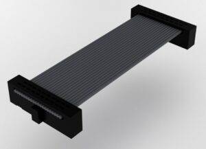
Suggested cable mates include:
- FFSD-05-D-06.00-01-N – 6” IDC Ribbon Cable Assembly
- FFSD-05-D-12.00-01-N – 12” IDC Ribbon Cable Assembly
Other Samtec products that are compliant with JTAG:
- EJH: .100″ shrouded IDC ejector header
- FTSH: .050″ terminal strip
- HHSC: .100″ JTAG ribbon coax cable assembly
- TST: .100″ shrouded terminal strip, mates with HHSC cable
- TSW: .100″ terminal strip
Embrace the Power of JTAG
JTAG remains a valuable tool for testing, programming, and debugging embedded systems. Its flexibility and standardization make it a cornerstone technology in the world of electronics development.